Dr. Hong Xiao
Sr. E-beam and Processing Expert
SPIE Involvement:
Author | Instructor
Area of Expertise:
Semiconductor manufacturing process technologies , Electron beam defect inspection , Electron beam defect review , Applications of SEM in IC chip manufacturing , IC chip manufacturing technology trends
Profile Summary

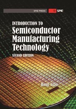
Dr. Hong Xiao is the Sr. e-beam and processing expert of ASML with expertise in e-beam applications in defect inspection, defect review, and CDU and overlay metrologies of IC chip manufacturing processes. He worked as e-beam technologist of KLA Corp.; technical marketing specialist of Hermes-Microvision, Inc.; and technical manager of Hermes Epitek Corp. He was a Sr. process engineer in Motorola; associate professor of Austin Community College; and Sr. technical instructor of Applied Materials. He received the Ph.D. in physics from the University of Texas at Austin, Dr. Xiao authored and co-authored over 30 journal and conference papers. He has more than 30 patents in US and other countries. He is the author of textbooks, “Introduction to Semiconductor Manufacturing Technology” the 2nd edition published by SPIE Press in Dec. 2012 and “3D IC Devices, Technologies, and Manufacturing” published by SPIE Press in 2016. He is a member of SPIE since 2005 and lifetime member of Chinese American Semiconductor Professional Association.
Publications (16)

SPIE Press Book | 29 April 2016
KEYWORDS: Photomasks, Etching, Silicon, Oxides, Semiconducting wafers, Metals, Dielectrics, Tin, Manufacturing

Proceedings Article | 18 April 2013 Paper
Hong Xiao, Ximan Jiang, David Trease, Mike Van Riet, Shishir Ramprasad, Anadi Bhatia, Pierre Lefebvre, David Bastard, Olivier Moreau, Chris Maher, Paul MacDonald, Cecelia Campochiaro
Proceedings Volume 8681, 86810F (2013) https://doi.org/10.1117/12.2011162
KEYWORDS: Copper, Metals, Scanning electron microscopy, Semiconducting wafers, Monte Carlo methods, Tungsten, Virtual colonoscopy, Transmission electron microscopy, Inspection, Chemical mechanical planarization

SPIE Press Book | 19 November 2012
KEYWORDS: Semiconducting wafers, Etching, Silicon, Oxides, Metals, Dielectrics, Ions, Plasma, Copper, Photoresist materials

Proceedings Article | 28 April 2011 Paper
Jennifer Fullam, Carol Boye, Theodorus Standaert, John Gaudiello, Derek Tomlinson, Hong Xiao, Wei Fang, Xu Zhang, Fei Wang, Long Ma, Yan Zhao, Jack Jau
Proceedings Volume 7971, 79710Y (2011) https://doi.org/10.1117/12.879910
KEYWORDS: Critical dimension metrology, Semiconducting wafers, Scanning electron microscopy, Inspection, Electron microscopes, Defect inspection, Data acquisition, Etching, Field effect transistors

Proceedings Article | 7 April 2011 Paper
Proceedings Volume 7969, 79691B (2011) https://doi.org/10.1117/12.879565
KEYWORDS: Inspection, Extreme ultraviolet, Photomasks, Extreme ultraviolet lithography, Defect detection, Lithography, Manufacturing, Particles, Electronic components, Opacity

Showing 5 of 16 publications
Course Instructor
SC1009: Introduction to Scanning Electron Microscope (SEM) Applications of Defect Inspection and Review in IC Manufacturing
This course explains basic principles and applications of defect electron beam inspection (EBI) and defect e-beam review (EBR). The primary goals of the course are to describe the basic of SEM imaging, defect behavior in the SEM image, case studies of EBI and EBR applications in semiconductor process development and high-volume manufacturing (HVM). Basics principles of design for inspection (DFI) and some case studies of EBI test circuit design are also covered.
SIGN IN TO:
  • View contact details

UPDATE YOUR PROFILE
Is this your profile? Update it now.
Don’t have a profile and want one?

Advertisement
Advertisement
Back to Top