
|
|
1.IntroductionQuantum wells (QW), quantum dots (QD), and other nanoscale devices created new possibilities for the development of microelectronics and microoptics. One of the promising approaches is based on photonic crystals, allowing the control of dispersion and propagation of light.1,2 The best-known effects include transmission or rejection of light in a given wavelength range and waveguiding the light along linear and bent defects in a periodic photonic crystal structure. A surface plasmon is a transverse magnetic-polarized optical surface wave that propagates along a metal-dielectric interface. Surface plasmons exhibit a range of interesting and useful properties, such as energy asymptotes in the dispersion curves, resonances, field enhancement and localization, high surface and bulk sensitivities to absorbed molecules, and subwavelength confinement. Because of these attributes, surface plasmons found applications in a variety of areas such as spectroscopy, nanophotonics, imaging, biosensing, and circuitry.3–10 Plasmon theory was extensively used to interpret the phenomena of light focusing at the nanoscale.11–34 Technical applications of the optical nanodevices have also been widely discussed,35–74 with several examples of natural nanostructures for light harvesting, transmission, and reflection described in plants and bacteria.75,76 Specific filament-like biological nanostructures were described as necessary for the transparency of the vertebrate crystalline lens. The lens in the vertebrates is built of the so-called fiber cells; these cells are very narrow (3 to ) and very long (millimeters), thus resembling fibers.77 These cells have specialized beaded intermediate filaments (IFs) 10 to 15 nm in diameter, built of proteins filensin and phakinin. Such fibers were described as indispensable for the fiber cell transparency, with many alterations to these IFs of chemical or genetic origin resulting in the lens cataract formation.78–86 Recently, a high level of transparency was also described in certain retinal cells. It was shown that light transmission in the vertebrate retina is restricted to specialized glial cells, which have many other physiological functions. Indeed, Franze et al.87 in their pioneering studies demonstrated that the Müller glial cells function as optical fibers. They demonstrated that Müller cells (MCs) transmit visible-range photons from the retinal surface to the photoreceptor cells, located deep under the surface. In fact, the retina has inverted structure, thus the light projected onto it has to pass through several layers of randomly oriented cells with intrinsic scatterers before it reaches the light-detecting photoreceptor cells.88,89 However, the guinea pig retina contains a regular pattern of MCs arranged mostly in parallel to each other, spanning the entire thickness of the retina ( to ). The MC main cylindrical process90 that spans the retina resembles an optical fiber, because of its capacity to transmit light.87 These cells typically have several complex side branches with functions not related to light transmission, with variable morphology.90,91 Thus, the main processes of the MCs create a way for the light to go through the retina. Here, we suggest that these main processes may contain specialized molecular structures functioning as optical waveguides. Therefore, it is important to investigate the morphology of the MCs main processes and develop a theoretical model of light transmission by these cells. Numerous materials form dielectric-conductive waveguides, including carbon-based materials with high carrier mobility and conductivity.92 Presently, we shall interpret the light transmission by MCs87 based on the model of light transmission by a waveguide with conductive nanolayer coating. A dielectric waveguide with a metal nanolayer coating is adequately described by the plasmon theory.1–10 This theory uses the quantum electronics approach to analyze the electromagnetic field (EMF) energy transmission by such a waveguide. A plasmon is understood as a conduction-band electron oscillation along the waveguide surface at the external EMF frequency.3–8,16–21,53–69 Such oscillations are induced by the EMF at the input end of the waveguide, and then the plasmon energy is transformed back into the EMF at the output end of the waveguide.3–8,16–21,53–69 Presently, we shall focus our attention on the role of the quantum confinement (QC) in the light transmission by MCs and nanotubes with a conductive coating, where the QC operates in the direction normal to the coating. We will analyze the EMF-induced transitions between the discrete states created in the conductive coatings, and the excitation transport from the input end of the waveguide to its output end. We shall demonstrate that the excitation transport should operate simultaneously with the state-to-state transitions, as the ground- and excited-state wavefunctions span the entire surface of the nanocoating. Now, we extend this approach to the analysis of the light transmission by the MCs, proposing a mechanism describing this phenomenon. This study has a direct impact on the medicine of human vision, and also on the development of nanomedical eye technology. 2.Experimental Methods and MaterialsThe presently used histological material was collected in Russia in 1999 during the study of the bifoveal retina of the pied flycatcher (Ficedula hypoleuca). The eyeballs of the flycatcher chicks 27 days after hatching were fixed in 3% gluteraldehyde with 2% paraformaldehyde in 0.15 M cacodilate buffer and postfixed with 1% in the same buffer. The eyeballs were oriented relative to the position of the pecten and embedded into Epon-812 epoxy resin. Ultrathin sections 60-nm thick were made on an LKB Bromma Ultratome ultramicrotome (L.K.B. Instruments Ltd., Northampton, United Kingdom) and examined on a JEM 100B (JEOL Ltd., Japan) electron microscope as described earlier.93 3.Experimental ResultsThe MCs in a Pied flycatcher eye extend from the vitreous body, where the light is entering the retina, through the entire retina to the photoreceptor cone cells, and thus the cell structure resembles the one previously described in the guinea pig eye.87 The MC bodies are located in a specific layer inside the retina, sending the principal processes to both of its surfaces. Indeed, the electronic micrograms show that the MC endfeet (inverted cone-shaped parts of the MC covering the vitreous body, see Fig. 1, red arrows) form the inner surface lining called the inner limiting membrane (ILM), covering the entire inner surface of the retina. The basal processes of the MCs originating from the endfeet [Fig. 1(a), green arrows] protract away from the inner surface, normally to it and essentially parallel to each other [Fig. 1(a), green arrows], and spreading around branches of other cells. We suggest that similar to what was found in the guinea pig,87 the light incident from the vitreous body is entering the endfeet [Fig. 1(a), red arrows], and next the excitation energy flows from the basal process to the cell body to the apical processes, where it is transferred to the cone photoreceptor outer segment, as shown in Fig. 1(c). The diameter of the MC main process in the Pied flycatcher may be [Fig. 1(a)]; therefore, these cells working as waveguides should be described as natural nano-optical structures. Fig. 1(a) Endfeet (red arrows) and basal processes (green arrows) of MCs in the Pied flycatcher retina. (b) High magnification insert from (a), showing a part of cytoplasmic structure (green arrows) that has parallel linear elements resembling IFs. This structure spans the cytoplasm from the narrow part of the basal endfoot to the apical end that wraps around a cone photoreceptor, in the direction of light transmission. Scale bar in (a) and (b) is 500 nm. (c) Schematic presentation of the MCs (green arrows) with their endfeet (red arrows) and the cone photoreceptors (R, G, B). The light propagation direction coincides with the red arrows. 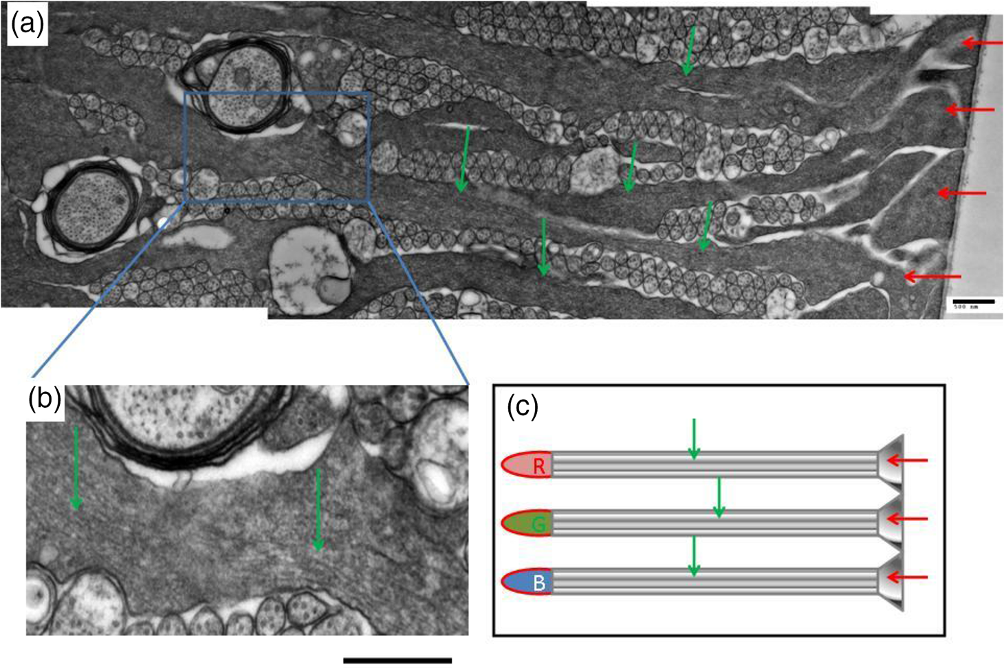 We also studied the cytoplasm of the MCs in the apical and basal processes, discovering parallel structures that span the cell cytoplasm all the way through from the inner membrane to the photoreceptors. A higher magnification insert of a part of the basal process of the MC87 [see Fig. 1(b)] shows this structure within the cytoplasm of the cell process, repeating all of its curves. This structure resembles a bundle of parallel IFs with the outer diameter of 10 nm, with some smaller microparticles organized around the filaments. The IFs in the glial cytoplasm are most often associated with globular particles of chaperone proteins (usually termed crystallines)94 that stabilize these long filaments, or with nucleoprotein particles.95 These filaments span almost the entire 400 to of the MC length, from the endfoot to the photoreceptor (the outer membrane), thus recalling the previous observations in other species.96 The filamentary structure is absent in the MC endfeet. Unfortunately, neither the precise ultrastructure of this intermediate-filament bundles in the MCs nor the continuity of the filaments, which may be important for understanding the mechanism of their operation, could be resolved on the presently used equipment, and will be investigated additionally. Usually, the IFs have their external diameter varying within 8 to 13 nm, with each filament typically built of eight protofibrils.97 Such specific IFs in the lens fiber cells are apparently responsible for the optical transparency of these cells.78–86 In our opinion, the bundles of IFs in the MCs of the Pied flycatcher eye are the structures responsible for the transmission of luminous energy to the photoreceptor cells, deserving a close attention of quantum physics. 4.Theoretical ModelsHere, we will discuss the (1) quasiclassical and (2) QC approaches to the analysis of light transmission by the IFs in MCs. The two approaches may be summarized as follows:
4.1.Quasiclassical ApproachWe already mentioned numerous studies1–74 that developed the theory of plasmonic quantum electronics and its applications to dielectric-conductive waveguides. Figure 2 shows this model schematically, where only the component of the electric field may produce plasmons, exciting electronic oscillations polarized along the surface of the waveguide. Fig. 2Schematic presentation of the input section of the lightguide with a nanothick conductive wall. is the Poynting vector, is the electric field vector of the incident EMF, is its magnetic field vector. 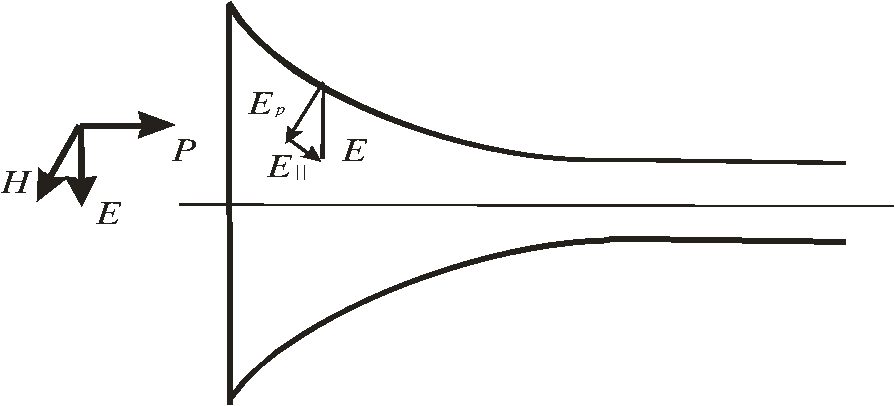 The efficiency of the energy transmission by a waveguide is significantly dependent on the profile of its input zone.3–18,64–74 Presently, however, we shall not discuss the plasmonic theory in detail, focusing our attention on the more exact quantum approach. 4.2.Quantum ConfinementAnalyzing tubes with nanometer-thick conductive walls, we must take into account the QC,92,98,99 appropriate for the light transmission by tubes with the diameter smaller than the wavelength of light. As we already mentioned, the parallel electric field component contributes to the plasmonic excitations, whereas the normal component contributes to exciting the discrete states created by the QC in the tube nanowalls. Thus, we shall consider the interaction of these field components with the respective quasicontinuum and discrete electronic states, followed by the EMF emission at the other end of the waveguide. The theoretic analysis of the QC in the device shown in Fig. 1 is very complex. Therefore, we simplified the system by considering a cylinder with the internal diameter , wall thickness , and length . The cylinder is linked to a cone, with the wall thickness , height , and aperture . Still, the problem admits numerical solutions only, with the results that we shall discuss next. We shall assume that the wavefunction amplitude is continuous at the contact surfaces between the cylinder and the two cones (see Fig. 3). Thus, we shall analyze the excitation at the input cone, the excitation transport via the cylinder, and the emission at the output cone, for the sake of symmetry. Fig. 3The model for qualitative analysis. The waveguide is composed of a tube and two cones, with conductive walls. 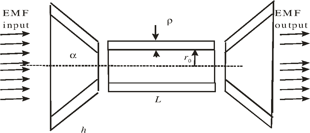 To evaluate these phenomena qualitatively, we need to determine the quantum states in the cylindrical part using cylindrical coordinates, and the quantum states in the conical part using conical coordinates. It is impossible to solve the Schrödinger equation analytically in a conical system, which we shall, therefore, analyze approximately. We shall also assume an increased excited-state population density in the output conical piece (the right side of the diagram) as compared to the input conical piece (the left side of the diagram). Thus, the energy transport in the model system reproduces the phenomena occurring in nature, where the excitation ends up on the chromophore molecules contained in the cone photoreceptor cells, with the higher excited-state density in the chromophores modeled by that in the output conical piece. 4.2.1.Cylindrical coordinatesWe solved the eigenstate problem for the conductive nanolayers, using the Schrödinger equation in the cylindrical coordinates (Appendix A). To this end, we used the boundary conditions equivalent to an axial potential box with infinite potential walls, an acceptable approximation for qualitative analysis. Generally, the Schrödinger equation in cylindrical coordinates reads where and is the effective electron mass. A detailed analysis of this equation is presented in Appendices A and B. The emission intensity at the output end of our axisymmetric system may be written in the dipole approximation as follows: where is the matrix element of the optical dipole–dipole transition. We shall further use Eq. (3) in the approximate numerical analysis of the light transmission by the IFs.4.2.2.Qualitative analysis of the solutions at the input and output conesMaking use of the axial symmetry of the system, we shall use the cylindrical coordinates. Appendix C presents the secular equation (SE) and the respective boundary conditions. It is possible to solve the SE only numerically, although we may obtain some qualitative results even without solving it. Next, we present the numerical results for the light transmission by the system of Fig. 4. In the input cone (Fig. 3), the electric field component interacts with the internal conical surface, exciting both longitudinal and transverse states. A detailed analysis of the energy transmission coefficient for the device shown in Fig. 3 is presented in Appendix D, with the resulting coefficient given by (see Appendix D) Fig. 4The model for numerical analysis, showing a cross section of the waveguide with conductive walls. is the curvature radius referred to in Fig. 5 and 6. 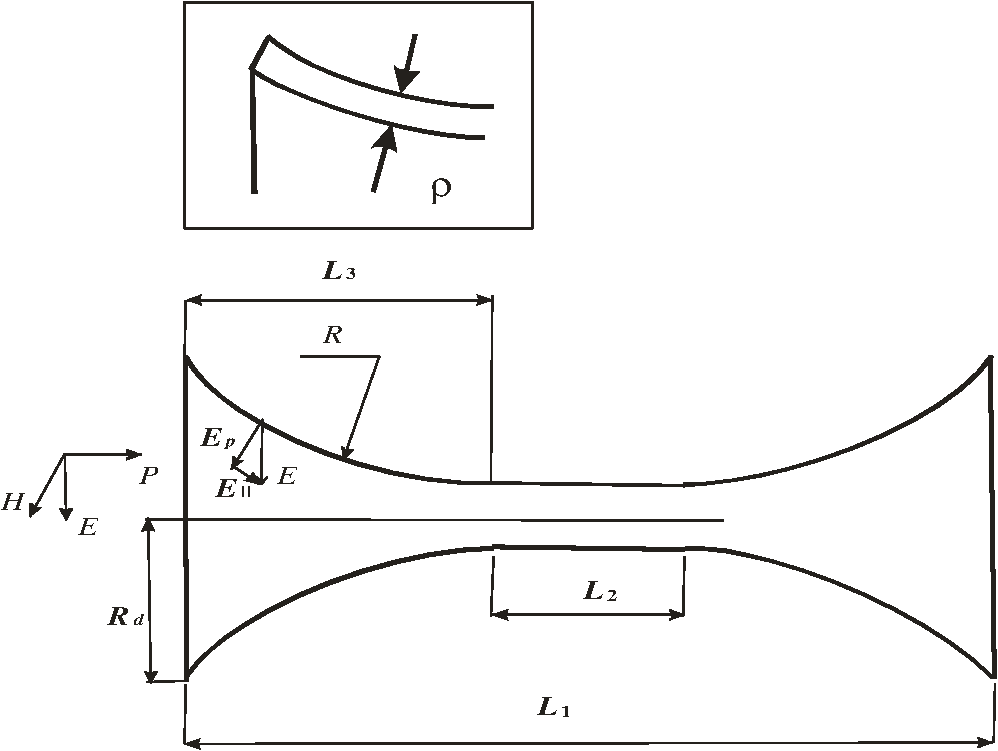 Equation (4) gives the light transmission efficiency as determined by the QC mechanism. In Sec. 4.2.3, we will carry out the numerical analysis of the QC effects for the device shown in Fig. 4. 4.2.3.Numerical analysis of the light transmission by the device of Fig. 4All parameters used for numerical analysis are listed in Table 1 and shown in Fig. 4. Table 1Parameters used in the numerical analysis.
Figure 4 shows the relevant geometrical parameters of the device. The internal diameter of the cylindrical tube is , and its wall thickness is , the same as that of the conical pieces. The length of the cylindrical tube is , the length of the entire device is , the length of the input and output pieces is , and is the curvature radius of the curved conical pieces. We shall assume that . The larger radius of the input and output cones is calculated as follows (Fig. 4): The boundary ring shown in the zoom-in box in Fig. 4 is normal to both the internal and the external limiting surfaces. Due to the axial symmetry of the system, we shall obtain the numerical solution of the SE in the cylindrical coordinates (see Appendix E). Since specific boundary conditions are created in the system considered (Fig. 4), the absorbed EMF energy is reemitted by the electronic excited states mainly in the output zone. This result is similar to the superemission observed in an active lasing medium. However, the similarity is only indirect, as it is impossible to create an inverse population distribution by an optical transition between the ground and the excited state. We shall address the spectral selectivity of the device in a follow-up publication. 4.3.Numerical CalculationsNumerical analysis was carried out using homemade FORTRAN software and the method of finite differences.100 We solved the Eqs. (26) and (30) numerically using and several different sets of the parameter values: ; , , , and ; ; ; ; (see Fig. 4). We used the following values of the size multipliers: , , and . We present the results in terms of the absorption efficiency where is the EMF intensity incident within the device cross sectionWe obtained the numerical solution of Eq. (76) using the finite difference method.100 We used a homemade FORTRAN code for the numerical analysis of this equation combined with Eqs. (80) and (7), with Fig. 5 showing the calculated results. Fig. 5Calculated plots of the transmission efficiency on the curvature radius (see Fig. 4). The values of the variable model parameters are: , (1) , (2) , (3) , and (4) . 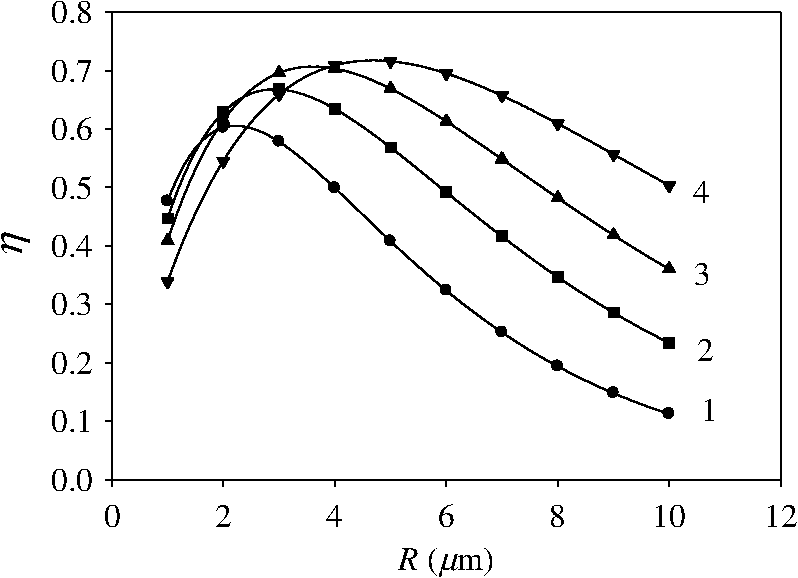 Figure 5 shows calculated plots of the transmission efficiency on the curvature radius (see Fig. 4). The values of the variable model parameters are: , (1) , (2) , (3) , and (4) . The efficiency of the light transmission varies with the geometry, with the maximum values corresponding to the following parameter sets: (1) , with the maximum cone radius ; (2) , ; (3) , ; (4) , . 4.4.On the Mechanism of Light Transmission by Müller CellsWe found that MCs contain internal longitudinal channels, with their diameter of around 10 nm, of unknown nature. As a hypothesis enabling the usage of the above mechanism, we shall assume that such channels have electrically conductive walls. Protein molecules are biologically viable building blocks for such conductive walls, as proteins have high electronic conductivity even in dry state, with the values approaching those typical for molecular conductors. These high values of the electrical conductivity apparently result from the existence of conjugated bonds in their structure, enabling high electronic mobility.101 However, in a simplified qualitative approach, we shall now consider the electronic states in a cylindrical carbon nanotube (CNT). 4.5.Electronic State Structure in a Carbon NanotubeWe shall start with a graphene monolayer, which has a conjugated π-system, with the energy gap between the bonding and antibonding/conductive zones vanishing asymptotically with the increasing system size.102 The local symmetry at each of the carbon atoms is , whereas the symmetry of the graphene elementary cell is . The macroscopic symmetry of the graphene sheet depends on its geometry. Presently, we shall analyze the effects of the local symmetry around a C atom. On each of the C atoms, there are three hybridized atomic orbitals located within the plane of the sheet, and one atomic orbital normal to the sheet.103 These orbitals form an orthonormalized set of states. In a CNT, the local symmetry around a C atom changes to , as three of the orbitals now form a pyramidal structure, with the pyramid height dependent on the CNT radius.103 Thus, the orbital is mixed with the other atomic states , their contribution increasing when the radius is reduced. The respective perturbation creates splitting between the bonding and antibonding/conductive zones, with the energy gap between these zones increasing for smaller values of the CNT radius.104 Similarly, the presence of O, S, N, P, and other heteroatoms affects the energy gap. The interaction with the EMF causes transitions to an excited state, with the excited-state wavefunction distributed over the entire CNT, which will facilitate the energy transport between the input and the output cones. Presently, we have no experimental evidence favoring this mechanism, which could explain the earlier reported light transmission by MCs.87 However, the MC structure as described in Sec. 3 is apparently compatible with the proposed mechanism, with the CNTs substituted by the protein fibers. Unfortunately, the structure of such protein fibers of the IFs is still unknown, thus we may only speculate that such proteins have a common conjugated -system similar to that of the CNTs. Therefore, the electronic excited states will have their excitation energy distributed over the entire conjugated -system of the molecule; thus, such a protein fiber may be excited at its input tip and then the excitation may lose its energy by emission at the output tip. Hence, good electric conductivity of the IF proteins is a necessary condition for the presently discussed mechanism, which we shall explore in our future studies.In Sec. 4.6, we present the results of the model calculations using , providing a better approximation to the geometry of the optical channels in the MCs (see Secs. 2 and 3). 4.6.Numerical Calculations for the Device with 0.5 nmWe carried out the model analysis for the following parameter values: ; , , , and ; ; ; ; , where , , and are the size multipliers. Note that this time the size multipliers have larger numeric values, so that the total channel lengths are similar: , , and , 200, 300, 400, 500, 600, 700, 700, 800, 900, and 1000. Figure 6 shows the numerical results. Here, all of the parameters , , , , , , , , and are the same as defined above. Fig. 6Calculated plots of the transmission efficiency on the curvature radius (see Fig. 4). The values of the variable model parameters are: , (1) , (2) , (3) , and (4) . 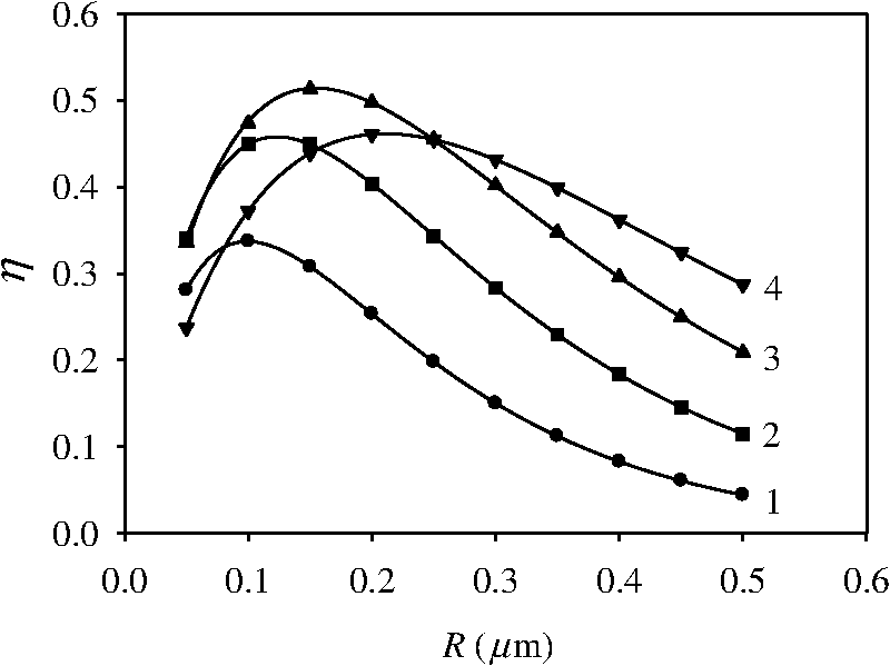 Once more, the EMF transmission efficiency has a maximum for each of the parameter sets, corresponding to the following values: (1) , ; (2) , ; (3) , ; and (4) , . As it follows from the results, the optimal radius of the input and the output sections () of the optical channels increases in comparison to the radius of the cylindrical section, while the difference decreases, all with the increasing . In effect, we obtain , with the overall geometry very similar to that of a cylindrical tube. However, the most notable result is the high efficiency of the EMF transmission by such small diameter channels, as obtained in the calculations. 4.7.Theoretical Description of the Absorption and Emission SpectraHere, we shall calculate the shape of the spectral band in the absorption/resonance emission spectrum. The shape of the spectral band is described by (see Appendix F) where Taking into account the algorithm developed above for the calculation of the transition matrix element , and using also we calculated the absorption band shape for the system of Fig. 4 using a home-made FORTRAN code with the following geometric parameters: , , , , and . The resulting spectrum is shown in Fig. 7.Fig. 7Calculated test absorption spectrum for device shown in Fig. 4, where the device parameters are: , , , , . 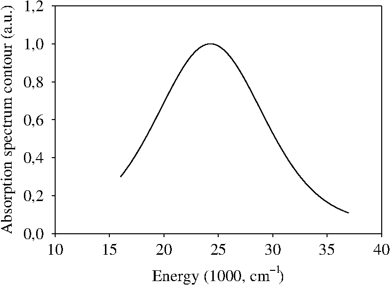 We see that the band maximum in Fig. 7 is located at , having the width of . A similar approach will be used in the follow-up papers to analyze the polarization selectivity105 and the spectral selectivity of the IFs. 5.DiscussionWe analyzed in detail the role of the QC in the transmission of the electromagnetic energy by axisymmetric nanochannels with conductive walls, the channel diameter much smaller than the wavelength of the electromagnetic radiation. Note that the transmission of the EMF by such structures may be described by the well-developed and frequently applied plasmon–polariton theory.1–37 The presently developed approach amounts to an extension of the plasmon–polariton theory in the QC limit.31,73 Indeed, we describe the quantum states in a waveguide built of nanostructured conductive materials. We assume that the interaction of the EMF with the waveguide produces a transition into the quantum excited state that is delocalized over the entire device, in agreement with the standard plasmon–polariton theory approach, where the energy of the EMF is transported within the waveguide in the form of excited-state electrons.1–8,42–72 However, there are some terminological differences; here, the excited state may be described as an exciton, whereas the plasmon–polariton theory describes such excited states as plasmons or polaritons. We presume that these are different designations for the same physical phenomena, resulting from different qualitative descriptions of the behavior of the system. The difference between the quasiclassical and QC approaches was discussed above, under “the theoretical model.” Both approaches describe the efficiency of the EMF energy transmission from the input section to the output section. The energy loss in both cases is determined by the energy relaxation processes. In the first model, these are described as friction exerted by the lattice on the electrons, whereas the second model describes radiationless relaxation due to exciton–phonon interaction. In both cases, the relaxation may be characterized by the phenomenological parameter , identical for the two models in the zero-order approximation. Therefore, both models should produce identical energy transmission efficiencies in the zero-order approximation, with any deviations appearing in higher orders only. We did not address this issue at this time. Presently, we analyzed a waveguide device with the same geometry of the input and the output sections. In principle, the energy transfer efficiency may depend on the geometry of each of these sections, thus allowing extra opportunities to optimize it. The optimum dimensions should also depend on the wavelength of the EMF, with a possibility of separate optimization for each of the color-vision photoreceptors. We shall explore these issues in a follow-up publication. Our main goal was to develop an understanding of the mechanisms of optical transparency of the MCs and other specialized transparent biological cells; next, we shall discuss the possible chemical composition of the waveguide structures. Note that protein molecules are universal structural building blocks in animal cells. Apparently, appropriate proteins may form the conductive walls of the nanostructured waveguides, as proteins have high electronic conductivity even in the dry state, with values approaching those of typical molecular conductors. These high values of electrical conductivity result from the existence of conjugated bonds in the structure of proteins, enabling high electronic mobility.102 Note that the experimental data and a quantum-mechanical model for the light transmission by CNTs, enabled by their conjugated -electron system, were reported by several authors.106,107 Their results correlate quite well with the conclusions derived from our present models. Still, the exact composition and structure of the specialized IFs in the MCs remain unknown, setting goals for future studies. Thus, as we already noted earlier,108 we should never overlook the direct transmission mechanism of luminous energy by biological nanostructures, including cellular IFs, based on their quantum nano-optical properties, along with the classical mechanisms reported earlier.83,109,110 Recently, Labin et al.111 considered light transmission by MCs using a classical model of a light guide that uses the difference between the refraction index of these cells and that of the surrounding medium to confine the light and guide it toward the light-sensitive cones. Interestingly, they also arrive at the conclusion that the light-transmission coefficient of the MC depends on the wavelength, with red and green light guided to the cones more efficiently than blue light. We find this result counter-intuitive, as generally it is more difficult to focus or guide the light with the larger wavelength (red) as compared to that with the shorter wavelength (blue), with a thicker waveguide required for the red light. All of the considerations presented here refer to conductive nanostructured IF bundles. Unfortunately, the structure and electric conductivity of the MC IFs remain unknown. However, the electric conductivity of different proteins was studied and reported earlier.101,112 Such electric conductivity of the polypeptide systems 101,112 was explained by their structure, including a common conjugated -system involving the entire length of the polypeptide molecule. We already mentioned that the electric conductivity is needed for our models to be valid. It was also shown113 that self-assembled monolayers formed by conformationally constrained hexapeptides are electrically conductive and generate photocurrent. Thus, peptide-based self-assembled monolayers efficiently mediate electron transfer and photoinduced electron transfer on gold substrates. These results112 may be described in terms of high electron mobility within the peptide monolayer in its electronic ground and excited states. We, therefore, infer that the IF polypeptides should be electrically conductive, enabling the presently proposed quantum mechanism as a complement and/or alternative to the classic mechanisms of the luminous energy transport within the retina. 6.ConclusionsIn this study, we report that MCs have long channels (waveguide structures), around 10 nm in diameter, spanning the larger part of the cell process, from the apex of the basal endfoot to the photoreceptor cells. Following the idea that such channels act as waveguides, we developed a QC model of the light transmission by the waveguides much thinner than the wavelength of the light quanta. We used our model for the qualitative analysis of the light transmission by such waveguides, with the calculations showing that such devices may transmit light with very high efficiencies from their input section to the output section, already possible in a device with a much simplified geometry. This mechanism was extended to the light transmission by the waveguides (specialized IFs) in the MCs, concluding that such waveguides are most probably built of proteins. Proteins have sufficient electric conductivity for the mechanism to be operational due to the presence of extended conjugated multiple bonds in their structure. The presently reported studies have a direct impact in the medicine of human vision and on the development of nanomedical vision technology. AppendicesAppendix AUsing cylindrical coordinates, the Laplace operator may be presented as follows: In Eq. (12), we may separate the radial and angular coordinates provided the wavefunction may be written as Thus, and Since we can writeThe latter may be rewritten as follows: The boundary conditions for the infinite-potential walls are Taking into account the boundary conditions, we conclude that the wavefunction is defined only in the interval. A.1.SolutionThe equation for the radial function may be written as For , we may write The solution of the latter equation may be presented as where are Bessel functions. For , the Bessel functions may be written asThus, the solution may be presented as follows: The latter relationship may be approximately presented as Taking into account the boundary condition ; , we obtain Thus, Taking into account the other boundary condition ; , we obtainThe latter equation cannot be solved directly, although it is apparent that the energy of the system states is a discrete function in the radial direction. To solve the equation we represent the radial function as follows: thus, our equation becomesTaking its derivative, we obtain Substituting we obtain which is equivalent to the equation obtained above. Since we may write Taking into account the solution for , we obtainTaking into account that we finally obtainFor the coordinate, we may write Assuming that at , we obtain Assuming now that at , we obtainThus, we finally obtain Appendix BThus, we wrote Eq. (22) as follows: Using the coordinate separation, we obtain We solve the above equations in Appendix A, with the result given by for the ground state, and for the excited states, where the quantization caused by the QC in the radial direction is described by The latter equation may be solved numerically to obtain the values of and hence the energies of the eigenstates. There is also the state quantization in the axial direction, although with much larger than the diameter the respective energy spectrum is a quasicontinuum We introduce , the quantum state widths, describing the excited state relaxation dynamics, including their radiative decay. Note that the component causes transitions within the quasicontinuum, whereas the component causes transitions within the radial discrete spectrum. Note also that the eigenvalues for the general wavefunction areGenerally, an eigenstate wavefunction involves the entire system; however, we may still evaluate the time evolution of an excited state as described next.99 To calculate the time-dependent probability of the excited state prepared in the initial moment of time, we calculate the square of the absolute value of the probability amplitude The probability amplitude is then where and Therefore, The phenomenological parameters and are, respectively, dependent on and , while and for the ground state. We shall discuss the transverse (in the radial direction) and the longitudinal (parallel to the cylinder axis) excited states. Provided the longitudinal excited state is unrelaxed , the probability to find the system in the transverse excited state isConversely, if the transverse excited state is completely relaxed, the probability to find the system in the longitudinal excited state is We conclude that the conductive nanolayer contains the total excitation energy immediately after the excitation, whereupon the excitation decays according to Eqs. (61)–(63). To analyze the energy transport, we shall next consider the absorption and the emission at the input and output cones, respectively.Appendix CThe Schrodinger equation may be written as where and coordinates may be separated from using the wavefunction in the formUsing the same approach as in Appendix A, we may write The boundary conditions for this problem may be written as Since the variables and do not separate in Eq. (66), the problem may be solved only numerically using the boundary conditions in Eq. (67). Appendix DThe energy absorbed upon excitation is proportional to where is the electric field amplitude spectrum of the EMF, , are the level densities of the ground and excited states, respectively. Here, we assume that the level density of the ground state is constant, while that of the excited state is dependent on ; , are the wavefunctions of the ground and excited states and is the vector of the electron location in the conductive nanolayer. The absorbed energy is then transferred to the cylindrical part; here, the probability of the excited-state wavefunction transmission (, the transmission coefficient) and reflection (, the reflection coefficient) depends on the angle . The transmitted energy has a maximum in function of , and, therefore, may be optimized. Similarly, we may describe the energy transmission to the output cone. The excited states in the output cone will emit with the same spectrum as that of the excitation, as the relaxation of the excited states is quite slow, compared to the excitation transfer in our model (Fig. 3). Generally, the transmission and reflection coefficients are, respectively,Here, ; , are real functions of , and , are the phase angles. Thus, the fraction of the absorbed energy transmitted to the excited states of the output cone is where , are the transmission coefficients from the input cone to the cylinder, and from the cylinder to the output cone, respectively. If , , andLet us consider the EMF emission by the output cone. Assuming two equivalent cones, the Poynting vector of the output EMF will be parallel to the input Poynting vector , and parallel to the axis of symmetry. Then, the density of the emission intensity is where where , are the radiationless relaxation width and the characteristic emission time, respectively. We assume that , because . Here, is the matrix element of the interaction coupling the emitting and the dark states in the system, and is the density of the dark states. Therefore, .Appendix ETo describe the interaction with the EMF, we present the linear momentum as follows: Here, is the vector potential. The potential must be zero inside the device, thus we rewrite the SE as Here, the first term in the Hamiltonian describes the motion of the electron in the nanolayer and the second—its interaction with the EMF. The second term describes a perturbation to the steady-state problem, describing mixing of the ground state with the excited states. Using the perturbation theory, we first obtain the states in absence of a perturbation Here, is the orbital momentum projection on the symmetry axis. The geometry of the device (Fig. 4) in conjunction with the condition of infinite potential on the walls determines the boundary conditions. Using these, we obtain the energies and the respective eigenvectors describing the unperturbed states. Next, we calculate the probability of the transitions induced by the EMF Here, , , and are the wave vectors of the ground and excited states, and of the incident EMF, respectively. We may then use the latter relationship and calculate the transition probability leading to the light emission in the output cone of the device.We present the vector potential as Here, . Since the Poynting vector points along the device axis, the electric and magnetic field vectors , are normal to it. Thus, and whereNote that we substituted the sum over the values in Eq. (80) by integration. We used Eq. (80) in numerical calculations of the energy transmission efficiency by the device, by the mechanism that involves absorption of a photon at the input cone, and its emission at the output cone. Note that in the numerical analysis, the matrix element was approximated by the term , which corresponds to the electric dipole approximation (see Appendix F). Appendix FUsing the fundamentals of the time-dependent perturbation theory, the probability of the EMF-induced transitions between the ground and excited electronic states in the dipole approximation may be presented as follows: where is the first-order coefficient of the time-dependent perturbation theory in the system eigenvector presentation, are the zero-order energies of the excited and ground states, respectively, is the relaxation rate of the electronic excited state. Thus, where Thus,The band shape is determined by the second term in the latter relationship, i.e., The latter relationship determines the spectral profiles of the absorption and resonance emission. AcknowledgmentsThe authors are grateful to PR NASA EPSCoR (NASA Cooperative Agreement NNX13AB22A) and the NIH Grant G12 MD007583 for the financial support of this study. L. V. Zueva was supported by Grant 16-14-10159 from the Russian Science Foundation. M.I. is grateful to Dr. S. Skatchkov, Dr. A. Savvinov, and Dr. A. Zayas-Santiago for stimulating discussions on the role of Müller cells in vision. ReferencesJ. D. Joannopoulus, R. D. Meade and J. N. Winn, Photonic Crystals. Molding the Flow of Light, 2nd ed.Princeton University Press, Princeton, New Jersey
(1995). Google Scholar
A. V. Zayats and I. I. Smolyaninov,
“Focusing and directing of surface plasmon polaritons by curved chains of nanoparticles,”
J. Opt. A: Pure Appl. Opt., 5 S16
–S50
(2003). http://dx.doi.org/10.1088/1464-4258/5/4/353 Google Scholar
F. R. Oulton et al.,
“Time-resolved surface plasmon polariton coupled exciton and biexciton emission,”
Nature, 461 629
–632
(2009). http://dx.doi.org/10.1038/nature08364 Google Scholar
P. L. Stiles et al.,
“Surface-enhanced Raman spectroscopy,”
Ann. Rev. Anal. Chem., 1 601
–626
(2008). http://dx.doi.org/10.1146/annurev.anchem.1.031207.112814 Google Scholar
W. L. Barnes, A. Dereux and T. W. Ebbesen,
“Surface plasmon subwavelength optics,”
Nature, 424 824
–830
(2003). http://dx.doi.org/10.1038/nature01937 Google Scholar
D. K. Gramotnev and S. I. Bozhevolnyi,
“Nanofocusing of electromagnetic radiation,”
Nat. Photonics, 4 83
–91
(2010). http://dx.doi.org/10.1038/nphoton.2009.282 NPAHBY 1749-4885 Google Scholar
S. Kawata, Y. Inouye and P. Verma,
“Nanofocusing of electromagnetic radiation,”
Nat. Photonics, 3 388
–394
(2009). http://dx.doi.org/10.1038/nphoton.2009.111 NPAHBY 1749-4885 Google Scholar
J. N. Anker et al.,
“Biosensing with plasmonic nanosensors,”
Nat. Mater., 7 442
–453
(2008). http://dx.doi.org/10.1038/nmat2162 NMAACR 1476-1122 Google Scholar
J. Homola,
“Surface plasmon resonance sensors for detection of chemical and biological species,”
Chem. Rev., 108 462
–493
(2008). http://dx.doi.org/10.1021/cr068107d CHREAY 0009-2665 Google Scholar
T. W. Ebbesen, C. Genet and S. I. Bozhevolnyi,
“Surface-plasmon circuitry,”
Phys. Today, 61 44
–50
(2008). http://dx.doi.org/10.1063/1.2930735 PHTOAD 0031-9228 Google Scholar
K. Okamoto et al.,
“Enhanced spontaneous emission inside hyperbolic metamaterials,”
Nat. Mater., 3 601
–605
(2004). http://dx.doi.org/10.1038/nmat1198 NMAACR 1476-1122 Google Scholar
R. F. Oulton et al.,
“Waveguide-fed optical hybrid plasmonic patch nano-antenna,”
Nature, 461 629
–632
(2009). http://dx.doi.org/10.1038/nature08364 Google Scholar
A. V. Akimov et al.,
“Generation of single optical plasmons in metallic nanowires coupled to quantum dots,”
Nature, 450 402
–406
(2007). http://dx.doi.org/10.1038/nature06230 Google Scholar
P. Neutens et al.,
“Electrical detection of confined gap plasmons in metal-insulator–metal waveguides,”
Nat. Photonics, 3 283
–286
(2009). http://dx.doi.org/10.1038/nphoton.2009.47 NPAHBY 1749-4885 Google Scholar
H. Ditlbacher et al.,
“Surface plasmon polariton microscope with parabolic reflectors,”
Phys. Rev. Lett., 95 257403
(2005). http://dx.doi.org/10.1103/PhysRevLett.95.257403 PRLTAO 0031-9007 Google Scholar
D. K. Gramotnev and S. I. Bozhevolnyi,
“Plasmonics beyond the diffraction limit,”
Nat. Photonics, 4 83
–91
(2010). http://dx.doi.org/10.1038/nphoton.2009.282 NPAHBY 1749-4885 Google Scholar
P. Berini,
“Hollow hybrid plasmonic waveguide for nanoscale optical confinement with long-range propagation,”
J. Appl. Phys., 102 033112
(2007). http://dx.doi.org/10.1063/1.2764222 JAPIAU 0021-8979 Google Scholar
Y. H. Joo et al.,
“Hollow hybrid plasmonic waveguide for nanoscale optical confinement with long-range propagation,”
Appl. Phys. Lett., 92 161103
(2008). http://dx.doi.org/10.1063/1.2913015 APPLAB 0003-6951 Google Scholar
A. Hosseini, H. Nejati and Y. Massoud,
“Design of a maximally flat optical low pass filter using plasmonic nanostrip waveguides,”
Opt. Express, 15 15280
–15286
(2007). http://dx.doi.org/10.1364/OE.15.015280 OPEXFF 1094-4087 Google Scholar
H. Lee, J. Song and E. Lee,
“An effective excitation of the lightwaves in the plasmonic nanostrip by way of directional coupling,”
J. Korean Phys. Soc., 57 1577
–1580
(2010). http://dx.doi.org/10.3938/jkps.57.1577 KPSJAS 0374-4884 Google Scholar
J. Song et al.,
“Nanofocusing of light using three-dimensional plasmonic mode conversion,”
J. Korean Phys. Soc., 57 1789
–1793
(2010). http://dx.doi.org/10.3938/jkps.57.1789 KPSJAS 0374-4884 Google Scholar
D. F. P. Pile et al.,
“On long-range plasmonic modes in metallic gaps,”
J. Appl. Phys., 100 013101
(2006). http://dx.doi.org/10.1063/1.2208291 JAPIAU 0021-8979 Google Scholar
G. Veronis and S. Fan,
“Theoretical investigation of compact couplers between dielectric slab waveguides and two-dimensional metal-dielectric-metal plasmonic waveguides,”
Opt. Lett., 30 3359
–3361
(2005). http://dx.doi.org/10.1364/OL.30.003359 OPLEDP 0146-9592 Google Scholar
G. B. Hoffman and R. M. Reano,
“Investigation of coupling length in a semi-cylindrical surface plasmonic coupler,”
Opt. Express, 16 12677
–12687
(2008). http://dx.doi.org/10.1364/OE.16.012677 OPEXFF 1094-4087 Google Scholar
B. Wang and G. P. Wang,
“Squeezing light into subwavelength metallic tapers: single mode matching method,”
Opt. Lett., 29 1992
–1994
(2004). http://dx.doi.org/10.1364/OL.29.001992 OPLEDP 0146-9592 Google Scholar
P. Ginzburg, D. Arbel and M. Orenstein,
“Gap plasmon polariton structure for very efficient microscale-to-nanoscale interfacing,”
Opt. Lett., 31 3288
–3290
(2006). http://dx.doi.org/10.1364/OL.31.003288 OPLEDP 0146-9592 Google Scholar
H. Choi et al.,
“A hybrid plasmonic waveguide for subwavelength confinement and long-range propagation,”
Opt. Express, 17 7519
–7524
(2009). http://dx.doi.org/10.1364/OE.17.007519 OPEXFF 1094-4087 Google Scholar
V. S. Volkov et al.,
“Channel plasmon polaritons guided by graded gaps: closed-form solutions,”
Nano Lett., 9 1278
–1282
(2009). http://dx.doi.org/10.1021/nl900268v NALEFD 1530-6984 Google Scholar
S. Vedantam et al.,
“A plasmonic dimple lens for nanoscale focusing of light,”
Nano Lett., 9 3447
–3452
(2009). http://dx.doi.org/10.1021/nl9016368 NALEFD 1530-6984 Google Scholar
E. Verhagen, L. K. Kuipers and A. Polman,
“Teardrop-shaped surface-plasmon resonators,”
Nano Lett., 10 3665
–3669
(2010). http://dx.doi.org/10.1021/nl102120p NALEFD 1530-6984 Google Scholar
S. I. Bozhevolnyi and K. V. Nerkararyan,
“Adiabatic nanofocusing of channel plasmon polaritons,”
Opt. Lett., 35 541
–543
(2010). http://dx.doi.org/10.1364/OL.35.000541 OPLEDP 0146-9592 Google Scholar
M. Schnell et al.,
“Plasmonic mode converter for controlling optical impedance and nanoscale light-matter interaction,”
Nat. Photonics, 5 283
–287
(2011). http://dx.doi.org/10.1038/nphoton.2011.33 NPAHBY 1749-4885 Google Scholar
M. I. Stockman,
“Nanofocusing of optical energy in tapered plasmonic waveguides,”
Phys. Rev. Lett., 93 137404
(2004). http://dx.doi.org/10.1103/PhysRevLett.93.137404 PRLTAO 0031-9007 Google Scholar
H. Choo et al.,
“Nanofocusing in a metal–insulator–metal gap plasmon waveguide with a three-dimensional linear taper,”
Nat. Photonics, 6
(12), 838
–844
(2012). http://dx.doi.org/10.1038/nphoton.2012.277 NPAHBY 1749-4885 Google Scholar
E. Ozbay,
“Plasmonics: merging photonics and electronics at nanoscale dimensions,”
Science, 311 189
–193
(2006). http://dx.doi.org/10.1126/science.1114849 SCIEAS 0036-8075 Google Scholar
M. J. Kobrinsky et al.,
“Hybrid III-V semiconductor/silicon nanolaser,”
Intel Technol. J., 8 129
–141
(2004). http://dx.doi.org/10.1364/OE.19.009221 Google Scholar
R. H. Ritchie,
“Plasma losses by fast electrons in thin films,”
Phys. Rev., 106 874
–881
(1957). http://dx.doi.org/10.1103/PhysRev.106.874 PHRVAO 0031-899X Google Scholar
W. L. Barnes, A. Dereux and T. W. Ebbesen,
“Review article: surface plasmon subwavelength optics,”
Nature, 424 824
–830
(2003). http://dx.doi.org/10.1038/nature01937 Google Scholar
S. A. Maier and H. A. Atwater,
“A Kirchhoff solution to plasmon hybridization,”
J. Appl. Phys., 98 011101
(2005). http://dx.doi.org/10.1063/1.1951057 JAPIAU 0021-8979 Google Scholar
S. A. Maier, Plasmonics Fundamentals and Applications, 21
–34 1st ed.Springer, New York
(2007). Google Scholar
S. Lal, S. Link and N. Halas,
“Nanooptics from sensing to waveguiding,”
Nat. Photonics, 1 641
–648
(2007). http://dx.doi.org/10.1038/nphoton.2007.223 NPAHBY 1749-4885 Google Scholar
V. G. Veselago,
“The electrodynamics of substances with simultaneously negative values of and ,”
Sov. Phys. Usp., 10 509
–514
(1968). http://dx.doi.org/10.1070/PU1968v010n04ABEH003699 PHUSEY 1063-7869 Google Scholar
J. B. Pendry,
“Negative refraction makes a perfect lens,”
Phys. Rev. Lett., 85 3966
–3969
(2000). http://dx.doi.org/10.1103/PhysRevLett.85.3966 PRLTAO 0031-9007 Google Scholar
W. Cai and V. M. Shalaev, Optical Metamaterials: Fundamentals and Applications, 1st ed.Springer, New York
(2009). Google Scholar
A. J. Ward and J. B. Pendry,
“Design of electromagnetic refractor and phase transformer using coordinate transformation theory,”
J. Mod. Opt., 43 773
–793
(1996). http://dx.doi.org/10.1080/09500349608232782 JMOPEW 0950-0340 Google Scholar
J. B. Pendry, D. Schurig and D. R. Smith,
“Calculation of material properties and ray tracing in transformation media,”
Science, 312 1780
–1782
(2006). http://dx.doi.org/10.1126/science.1125907 SCIEAS 0036-8075 Google Scholar
A. V. Kildishev and V. M. Shalaev,
“Engineering space for light via transformation optics,”
Opt. Lett., 33 43
–45
(2008). http://dx.doi.org/10.1364/OL.33.000043 Google Scholar
V. M. Shalaev,
“Optical source transformations,”
Science, 322 384
–386
(2008). http://dx.doi.org/10.1126/science.1166079 SCIEAS 0036-8075 Google Scholar
S. A. Maier et al.,
“Structural-configurated magnetic plasmon bands in connected ring chains,”
Nat. Mater., 2 229
–232
(2003). http://dx.doi.org/10.1038/nmat852 NMAACR 1476-1122 Google Scholar
S. I. Bozhevolnyi et al.,
“Channel plasmon subwavelength waveguide components including interferometers and ring resonators,”
Nature, 440 508
–511
(2006). http://dx.doi.org/10.1038/nature04594 Google Scholar
A. Rechberger et al.,
“Optical properties of two interacting gold nanoparticles,”
Opt. Commun., 220 137
–141
(2003). http://dx.doi.org/10.1016/S0030-4018(03)01357-9 OPCOB8 0030-4018 Google Scholar
D. P. Fromm et al.,
“Simplified model for periodic nanoantennae: linear model and inverse design,”
Nano Lett., 4 957
–961
(2004). http://dx.doi.org/10.1021/nl049951r NALEFD 1530-6984 Google Scholar
T. Atay, J. H. Song and A. V. Nurmikko,
“Strongly interacting plasmon nanoparticle pairs: from dipole–dipole interaction to conductively coupled regime,”
Nano Lett., 4 1627
–1631
(2004). http://dx.doi.org/10.1021/nl049215n NALEFD 1530-6984 Google Scholar
P. Muhlschlegel et al.,
“Resonant optical antennas,”
Science, 308 1607
–1609
(2005). http://dx.doi.org/10.1126/science.1111886 SCIEAS 0036-8075 Google Scholar
A. Sundaramurthy et al.,
“Full analytical model for obtaining surface plasmon resonance modes of metal nanoparticle structures embedded in layered media,”
Phys. Rev. B, 72 165409
(2005). http://dx.doi.org/10.1103/PhysRevB.72.165409 Google Scholar
A. K. Sarychev, G. Shvets and V. M. Shalaev,
“Doubly negative metamaterials in the near infrared and visible regimes based on thin film nanocomposites,”
Phys. Rev. E, 73 36609
(2006). http://dx.doi.org/10.1103/PhysRevE.73.036609 Google Scholar
A. Sundaramurthy et al.,
“Contact optical nanolithography using nanoscale C-shaped apertures,”
Nano Lett., 6 355
–360
(2006). http://dx.doi.org/10.1021/nl052322c NALEFD 1530-6984 Google Scholar
O. L. Muskens et al.,
“Strong enhancement of the radiative decay rate of emitters by single plasmonic nanoantennas,”
Nano Lett., 7 2871
–2875
(2007). http://dx.doi.org/10.1021/nl0715847 NALEFD 1530-6984 Google Scholar
R. M. Bakker et al.,
“Simplified model for periodic nanoantennae: linear model and inverse design,”
New J. Phys., 10 125022
(2008). http://dx.doi.org/10.1088/1367-2630/10/12/125022 NJOPFM 1367-2630 Google Scholar
R. M. Bakker et al.,
“Enhanced localized fluorescence in plasmonic nanoantennae,”
Appl. Phys. Lett., 92 043101
(2008). http://dx.doi.org/10.1063/1.2836271 APPLAB 0003-6951 Google Scholar
N. Fang and X. Zhang,
“Optical superlines,”
Appl. Phys. Lett., 82 161
–163
(2003). http://dx.doi.org/10.1063/1.1536712 APPLAB 0003-6951 Google Scholar
N. Fang et al.,
“Sub-diffraction-limited optical imaging with a silver superlens,”
Science, 308 534
–537
(2005). http://dx.doi.org/10.1126/science.1108759 SCIEAS 0036-8075 Google Scholar
D. O. S. Melville and R. J. Blaikie,
“Analysis and comparison of simulation techniques for silver superlenses,”
Opt. Exp., 13 2127
–2134
(2005). http://dx.doi.org/10.1364/OPEX.13.002127 OPEXFF 1094-4087 Google Scholar
W. Cai, D. A. Genov and V. M. Shalaev,
“Negative index metamaterial combining magnetic resonators with metal films,”
Phys. Rev. B, 72 193101
(2005). http://dx.doi.org/10.1103/PhysRevB.72.193101 Google Scholar
D. Schurig et al.,
“Metamaterial cloaks for EM wireless multi-channel telecommunication,”
Science, 314 977
–980
(2006). http://dx.doi.org/10.1126/science.1133628 SCIEAS 0036-8075 Google Scholar
U. Leonhardt,
“A novel refractive technique for achieving macroscopic invisibility of visual light,”
Science, 312 1777
–1780
(2006). http://dx.doi.org/10.1126/science.1126493 SCIEAS 0036-8075 Google Scholar
W. S. Cai et al.,
“Optical cloaking with metamaterials,”
Nat. Photonics Nat. Photonics, 1 224
–227
(2007). http://dx.doi.org/10.1038/nphoton.2007.28 Google Scholar
A. Alù and N. Engheta,
“Optical cloaking: a many-layered solution,”
Phys. Rev. Lett., 100 113901
(2008). http://dx.doi.org/10.1103/PhysRevLett.100.113901 PRLTAO 0031-9007 Google Scholar
Z. Jacob, L. V. Alekseyev and E. Narimanov,
“Optical hyperlens: far-field imaging beyond the diffraction limit,”
Opt. Exp., 14 8247
–8256
(2006). http://dx.doi.org/10.1364/OE.14.008247 OPEXFF 1094-4087 Google Scholar
A. Salandrino and N. Engheta,
“Far-field subdiffraction optical microscopy using metamaterial crystals: theory and simulations,”
Phys. Rev. B, 74 75103
(2006). http://dx.doi.org/10.1103/PhysRevB.74.075103 Google Scholar
Z. Liu et al.,
“Development of optical hyperlens for imaging below the diffraction limit,”
Science, 315 1686
–1686
(2007). http://dx.doi.org/10.1126/science.1137368 SCIEAS 0036-8075 Google Scholar
I. I. Smolyaninov, Y. J. Hung and C. C. Davis,
“Electromagnetic cloaking in the visible frequency range,”
Science, 315 1699
–1701
(2007). http://dx.doi.org/10.1126/science.1138746 SCIEAS 0036-8075 Google Scholar
D. Schurig, J. B. Pendry and D. R. Smith,
“Transformation designed optical elements,”
Opt. Exp., 15 14772
–14782
(2007). http://dx.doi.org/10.1364/OE.15.014772 OPEXFF 1094-4087 Google Scholar
Y. Xiong, Z. Liu and X. Zhang,
“Focusing light into deep subwavelength using metamaterial immersion lenses,”
Appl. Phys. Lett., 94 203108
(2009). http://dx.doi.org/10.1063/1.3141457 APPLAB 0003-6951 Google Scholar
J. Hsin et al.,
“Energy transfer dynamics in an RC-LH1–PufX tubular photosynthetic membrane,”
New J. Phys., 12 085005
(2010). http://dx.doi.org/10.1088/1367-2630/12/8/085005 NJOPFM 1367-2630 Google Scholar
P. Vukusic and J. R. Sambles,
“Photonic structures in biology,”
Nature, 424 852
–855
(2003). http://dx.doi.org/10.1038/nature01941 Google Scholar
S. Bassnett, Y. Shi and G. F. J. M. Vrensen,
“Biological glass: structural determinants of eye lens transparency,”
Phil. Trans. R. Soc. B, 366 1250
–1264
(2011). http://dx.doi.org/10.1098/rstb.2010.0302 PTRBAE 0962-8436 Google Scholar
J. Tagliavini, S. A. Gandolfi and G. Maraini,
“Cytoskeleton abnormalities in human senile cataract,”
Curr. Eye Res., 5 903
–910
(1986). http://dx.doi.org/10.3109/02713688608995170 Google Scholar
H. Bloemendal,
“Proctor lecture. Disorganisation of membranes and abnormal intermediate filament assembly lead to cataract,”
Invest. Ophthalmol. Visual Sci., 32 445
–55
(1991). Google Scholar
J. M. Marcantonio and G. Duncan,
“Calcium-induced degradation of the lens cytoskeleton,”
Biochem. Soc. Trans., 19 1148
–1150
(1991). http://dx.doi.org/10.1042/bst0191148 Google Scholar
N. S. Rafferty, K. A. Rafferty and S. Zigman,
“Comparative response to UV irradiation of cytoskeletal elements in rabbit and skate lens epithelial cells,”
Curr. Eye Res., 16 310
–319
(1997). http://dx.doi.org/10.1076/ceyr.16.4.310.10687 Google Scholar
H. Matsushima et al.,
“Loss of cytoskeletal proteins and lens cell opacification in the selenite cataract model,”
Exp. Eye Res., 64 387
–395
(1997). http://dx.doi.org/10.1006/exer.1996.0220 Google Scholar
J. I. Clark et al.,
“Lens cytoskeleton and transparency: a model,”
Eye, 13
(Pt 3b), 417
–424
(1999). http://dx.doi.org/10.1038/eye.1999.116 12ZYAS 0950-222X Google Scholar
A. Alizadeh et al.,
“Targeted deletion of the lens fiber cell-specific intermediate filament protein filensin,”
Invest. Ophthalmol. Visual Sci., 44 5252
–5258
(2003). http://dx.doi.org/10.1167/iovs.03-0224 Google Scholar
M. Oka et al.,
“The function of filensin and phakinin in lens transparency,”
Mol. Vision, 14 815
–822
(2008). Google Scholar
S. Song et al.,
“Functions of the intermediate filament cytoskeleton in the eye lens,”
J. Clin. Invest., 119 1837
–1848
(2009). http://dx.doi.org/10.1172/JCI38277 Google Scholar
K. Franze et al.,
“Müller cells are living optical fibers in the vertebrate retina,”
Proc. Natl. Acad. Sci. U. S. A., 104 8287
–8292
(2007). http://dx.doi.org/10.1073/pnas.0611180104 Google Scholar
A. Hammer et al.,
“Optical properties of ocular fundus tissue-an in vitro study using the double-integrating-sphere technique and inverse Monte Carlo simulation,”
Phys. Med. Biol., 40 963
–978
(1995). http://dx.doi.org/10.1088/0031-9155/40/6/001 PHMBA7 0031-9155 Google Scholar
J. J. Vos and M. A. Bouman,
“Contribution of the retina to entoptic scatter,”
J. Opt. Soc. Am., 54 95
–100
(1964). http://dx.doi.org/10.1364/JOSA.54.000095 Google Scholar
M. Schultze, Zur Anatomie und Physiologie der Retina, Cohen & Sohn, Bonn, Germany
(1866). Google Scholar
A. Reichenbach et al.,
“The structure of rabbit retinal Müller (glial) cells is adapted to the surrounding retinal layers,”
Anat. Embryol., 180 71
–79
(1989). http://dx.doi.org/10.1007/BF00321902 Google Scholar
P. R. West et al.,
“Searching for better plasmonic materials,”
Laser Photonics Rev., 4 795
–808
(2010). http://dx.doi.org/10.1002/lpor.v4:6 LPRAB8 1863-8880 Google Scholar
T. V. Khokhlova, L. V. Zueva and T. V. Golubeva,
“Stages of development of retinal photoreceptor cells in postnatal ontogenesis of the pied flycatcher Ficedula hypoleuca,”
J. Evol. Biochem. Physiol., 36
(4), 461
–470
(2000). http://dx.doi.org/10.1007/BF02736998 JEBPA9 0022-0930 Google Scholar
M. D. Perng et al.,
“Glial fibrillary acidic protein filaments can tolerate the incorporation of assembly-compromised GFAP-delta, but with consequences for filament organization and alphaB-crystallin association,”
Mol. Biol. Cell, 19 4521
–4533
(2008). http://dx.doi.org/10.1091/mbc.E08-03-0284 Google Scholar
P. Traub et al.,
“Colocalization of single ribosomes with intermediate filaments in puromycin-treated and serum-starved mouse embryo fibroblasts,”
Biol. Cell, 90 319
–337
(1998). http://dx.doi.org/10.1111/j.1768-322X.1998.tb01042.x Google Scholar
A. Reichenbach and A. Bringmann, Müller Cells in the Healthy and Diseased Retina, 35 Springer, New York
(2010). Google Scholar
A. C. Steven,
“Intermediate filament structure,”
Cellular and Molecular Biology of Intermediate Filaments, 233
–263 Springer(1990). Google Scholar
M. Tkach et al.,
“Quasistationary and quasifree electron states in opened quantum dots,”
Rom. J. Phys., 54 37
–45
(2009). Google Scholar
L. D. Landau and E. M. Lifshitz, Quantum Mechanics, Fizmatgis, Moscow
(1963). Google Scholar
E. B. Krissinel and N. V. Shohirev, Solution of Non Stationary Diffusion Equation by Finite Difference Method,
(1987). Google Scholar
I. Ron et al.,
“Proteins as solid-state electronic conductors,”
Acc. Chem. Res., 43 945
–953
(2010). http://dx.doi.org/10.1021/ar900161u ACHRE4 0001-4842 Google Scholar
A. Geim,
“Graphene: status and prospects,”
Science, 324 1530
–1534
(2009). http://dx.doi.org/10.1126/science.1158877 SCIEAS 0036-8075 Google Scholar
C. Riedl et al.,
“Quasi-free standing epitaxial graphene on SiC by hydrogen intercalation,”
Phys. Rev. Lett., 103 246804
(2009). http://dx.doi.org/10.1103/PhysRevLett.103.246804 PRLTAO 0031-9007 Google Scholar
The University of Manchester, Web site: The Story of Graphene, 2014,
(2014) http://www.graphene.manchester.ac.uk/explore/the-story-of-graphene/ October ). 2014). Google Scholar
I. Khmelinskii et al.,
“Model of polarization selectivity of the intermediate filament optical channels,”
Photonics Nanostruct. Fundam. Appl., 16 24
–33
(2015). http://dx.doi.org/10.1016/j.photonics.2015.08.001 Google Scholar
M. V. Moghaddam et al.,
“Photon-impenetrable, electron-permeable: the carbon nanotube forest as a medium for multiphoton thermal-photoemission,”
ACS Nano, 9 4064
–4069
(2015). http://dx.doi.org/10.1021/acsnano.5b00115 ANCAC3 1936-0851 Google Scholar
S. Motavas, A. Ivanov and A. Nojeh,
“The effect of light polarization on the interband transition spectra of zigzag carbon nanotubes and its diameter dependence,”
Physica E Low-Dimens. Syst. Nanostruct., 56 79
–84
(2014). http://dx.doi.org/10.1016/j.physe.2013.08.007 Google Scholar
L. Zueva et al.,
“Foveolar Müller cells of the pied flycatcher: morphology and distribution of intermediate 5 filaments regarding cell transparency,”
Microsc. Microanal., 22
(2), 379
–386
(2016). http://dx.doi.org/10.1017/S1431927616000507 MIMIF7 1431-9276 Google Scholar
G. B. Benedek,
“Theory of transparency of the eye,”
Appl. Opt., 10 459
–473
(1971). http://dx.doi.org/10.1364/AO.10.000459 Google Scholar
S. Johnsen,
“Hidden in plain sight: the ecology and physiology of organismal transparency,”
Biol. Bull., 201 301
–318
(2001). http://dx.doi.org/10.2307/1543609 Google Scholar
A. M. Labin et al.,
“Müller cells separate between wavelengths to improve day vision with minimal effect upon night vision,”
Nat. Commun., 5 4319
–4323
(2014). http://dx.doi.org/10.1038/ncomms5319 NCAOBW 2041-1723 Google Scholar
X. U. Haixia,
“An investigation of the conductivity of peptide nanosstructured hydrogels via molecular self-assembly,”
The University of Manchester for the degree of Doctor of Philosophy in the Faculty of Engineering and Physical Sciences, School of Materials,
(2011). Google Scholar
E. Gatto et al.,
“Electroconductive and photocurrent generation properties of self-assembled monolayers formed by functionalized, conformationally-constrained peptides on gold electrodes,”
J. Pept. Sci., 14 184
–191
(2008). http://dx.doi.org/10.1002/psc.v14:2 Google Scholar
BiographyVladimir Makarov has worked as a senior researcher at the Institute of Chemical Kinetics and Combustion, Novosibirsk, Russia; invited senior researcher at the Institute of Troposphareforschung, Leipzig, Germany; invited researcher at RIKEN and at the Laboratory of Photochemistry, Institute of Environmental Studies, Tzukuba, Japan, being presently employed as a professor at the Laboratory of Nanomaterials, University of Puerto Rico, USA. He has published 104 papers in peer-reviewed journals. Lidia Zueva received her MSc in biophysics at the Leningrad Polytechnic Institute, Russia, and her PhD in biology at the Sechenov Institute RAN, Russia. She is a leading researcher at the Sechenov Institute of Evolutionary Physiology and Biochemistry, St. Petersburg, Russia. She is a consultant in morphology methods at the University of Puerto Rico. Her research interests are spectral characteristics of vertebrate photoreceptor cells (MSP) and their fine structure (EM), color vision in vertebrates in function of photic environment, development of vision in ontogenesis. Tatiana Golubeva is a leading researcher at the Department of Vertebrate Zoology of the Lomonosov Moscow State University. She received her PhD in the Department of Physiology of Animals of the Moscow State University. Her research interests are peripheral hearing mechanisms and their development in birds, bird sensory systems, structure and function of retina, development of hearing, vision and thermoregulation in birds, acoustical and visual communication in endotherms. Elena Korneeva received her PhD in biology by the Moscow Pedagogical Institute in 1983. She is a leading researcher at the Institute of Higher Nervous Activity & Neurophysiology, Russian Academy of Sciences, Moscow, Russia. She has over 80 publications on structural and functional changes in avian nervous system during ontogeny, development of vision, and visually guided behavior in nestlings. Igor Khmelinskii received his PhD from the Institute of Chemical Kinetics and Combustion, Novosibirsk, Russia, in 1988. He has been affiliated with Universidade do Algarve, Faro, Portugal, since 1993, with over 150 papers published in peer-reviewed journals on topics ranging from physical chemistry to education to climate-related issues. Mikhail Inyushin received his PhD in neurophysiology from the Leningrad State University (1986) and worked as neuroscientist in Leningrad studying mollusk neuronal nets, till 1994. He has Industirual experience in Colombia, Venezuela, and Mexico. He has been affliated with Universidad Central del Caribe, Puerto Rico, since 2004 and as assistant professor since 2008, with a grant from NIH. His interests include biophysics of the glial-vascular interface, with the emphasis on cellular transport of molecules and energy. |


